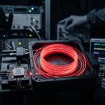
As artificial intelligence (AI) models expand into hundreds of billions—and soon trillions—of parameters, data centers face an unprecedented computational bottleneck. Traditional copper-based electrical interconnects are rapidly hitting their physical limits, constrained by severe signal attenuation, high latency, thermal dissipation, and restricted bandwidth density. To support the scale-up of generative AI, machine learning training clusters, and hyperscale cloud workloads, data transmission architectures must undergo a paradigm shift.
Enter AI Optical Interconnects—the critical optical infrastructure replacing legacy copper links to transport massive data streams between graphics processing units (GPUs), tensor processing units (TPUs), and high-performance switches at the speed of light. At the heart of this optical revolution lies the advanced VCSEL (Vertical-Cavity Surface-Emitting Laser) technology, specifically optimized at the 1060nm wavelength.
As a world-class manufacturer of advanced semiconductor lasers and optical lightsources, Inphenix delivers cutting-edge photonic solutions designed to empower next-generation data centers, telecommunications networks, and AI hardware ecosystems.
The AI Compute Crisis: Why AI Clusters Need Faster Optical Links
Modern AI workloads—such as large language models (LLMs), deep neural network (DNN) training, and real-time inference—require continuous, massive data exchanges across thousands of clustered processors. In a standard GPU cluster, nodes must synchronize parameters iteratively. When these communication pipelines are choked by electrical resistance and capacitive coupling in copper cables, processors spend idle clock cycles waiting for data. This phenomenon, known as the “memory wall” and “interconnect bottleneck,” severely degrades cluster efficiency and drives up energy consumption.
The Limitations of Copper
- Bandwidth Density: Copper traces and cables suffer from severe high-frequency attenuation, limiting maximum data rates over longer rack-to-rack spans.
- Power Dissipation and Thermal Management: Driving high-speed electrical signals across dense copper backplanes generates excessive heat, requiring effective thermal management and intensive cooling infrastructure.
- Reach and Latency: Electrical links degrade sharply beyond a few meters, forcing complex signal regeneration and introducing latency spikes.
The Optical Advantage
Transitioning to AI Optical Interconnects powered by silicon photonics eliminates these physical barriers, enabling every datacenter to support higher bandwidth and greater energy efficiency. By routing data via photons rather than electrons, data centers achieve terabits per second (Tbps) of throughput per fiber, ultra-low latency, and vastly superior energy efficiency per transmitted bit.
Decoding the Core Technology: The Rise of the VCSEL
While edge-emitting lasers and distributed feedback (DFB) lasers have traditionally anchored long-haul optical networks, short-to-medium reach data center fabrics—such as intra-rack, chip-to-chip, and co-packaged optics (CPO)—demand a different class of source: the VCSEL.
Unlike edge-emitters that emit light from the cleaved side of the semiconductor chip, a VCSEL emits a laser beam perpendicular to the top surface of the wafer. This unique architecture yields profound manufacturing and operational advantages:
- Wafer-Scale Testing: VCSEL wafers can be fully tested and burned-in prior to dicing, drastically reducing manufacturing costs and improving yield.
- Circular Beam Profile: The symmetric, circular output beam couples efficiently into standard multi-mode and single-mode optical fibers without requiring complex anamorphic lens systems.
- High Modulation Bandwidth: Modern designs support extreme direct modulation speeds exceeding 50 GBd and 100 Gbps per lane, making them ideal for high-density parallel optics.
- Low Power Consumption: Low threshold currents and high wall-plug efficiency translate to minimal thermal output within dense transceiver modules.
For designers looking to integrate specialized optical components, exploring industry-grade semiconductor solutions via Inphenix’s Product Catalogensures access to state-of-the-art packaging and custom wavelength specifications.
How 1060nm VCSELs Boost Bandwidth
For over two decades, short-reach optical interconnects relied heavily on 850nm GaAs-based VCSELs. While successful for legacy data rates (10G to 25G per channel), 850nm technology encounters significant physical limitations when pushed toward 100G+ per lane for modern AI clusters:
- Chromatic Dispersion: Higher dispersion in standard multi-mode fibers at 850nm limits reach and degrades high-frequency eye diagrams.
- Reliability at High Temperatures: Dense AI switch boards operate at elevated thermal loads, where traditional 850nm VCSEL reliability drops significantly.
Why 1060nm is the Sweet Spot for AI Clusters
Migrating the operating wavelength to 1060nm unlocks transformative performance gains for AI Optical Interconnects:
- Lower Fiber Attenuation and Dispersion: Multi-mode fibers exhibit significantly lower chromatic dispersion and attenuation closer to 1060nm compared to 850nm, enabling longer reach inside massive hyperscale facilities.
- Higher Operating Temperatures: 1060nm devices maintain exceptional slope efficiency and reliability under high-temperature, high-current injection conditions typical of dense GPU co-packaged optics.
- Extended Reach and Bandwidth: By pairing advanced 1060nm VCSELs with optimized optical fibers, data centers can scale link distances and support scale-up without sacrificing signal integrity.
To evaluate custom semiconductor laser options tailored for specific fiber-optic architectures, consult Inphenix’s Custom Service Portal.
Architectural Integration: Co-Packaged Optics and On-Board Photonics
As AI accelerators consume upwards of 1,000 watts per socket, traditional pluggable transceiver modules mounted on front panel faceplates introduce too much electrical trace loss from the ASIC switch chip to the front edge of the board in a datacenter.
The industry is rapidly transitioning toward Co-Packaged Optics (CPO) and Optical Compute Interconnects (OCI), where optical transceiver engines are placed directly on the same substrate or interposer as the AI processor.
[ AI GPU / ASIC ] <— Ultra-Short Electrical Trace —> [ 1060nm VCSEL Array Engine ] —> [ Optical Fiber Interconnect ]
In this architecture, VCSEL arrays are integrated directly alongside compute silicon, converting electrical tensor outputs directly into optical streams with near-zero trace loss. Inphenix supports this transition by engineering high-reliability laser diodes and optical components capable of meeting stringent telecommunication and datacom reliability standards (Telcordia GR-468).
Empowering the AI Ecosystem with Inphenix Photonics
Building reliable, high-speed AI Optical Interconnects requires uncompromising manufacturing precision, epitaxial expertise, and rigorous quality control. Inphenix stands at the forefront of the optoelectronics industry, offering a comprehensive portfolio of high-performance light sources.
Whether you are designing multi-terabit optical transceivers, co-packaged optics architectures, or advanced sensing modules, Inphenix provides end-to-end support—from custom wafer growth to advanced hermetic packaging. Discover how Inphenix accelerates optical innovation by reviewing Inphenix’s Technology Overview.
Conclusion
The exponential scaling of artificial intelligence is fundamentally redefining hardware design. As electrical interconnects reach their physical limits, AI Optical Interconnects driven by high-performance VCSEL technology—particularly optimized at 1060nm—provide the high-bandwidth, low-latency pathway required to sustain future computational demands.
By eliminating bottlenecks, reducing power consumption, and enabling massive parallel data streams, optical interconnects ensure that the hardware powering tomorrow’s AI can keep pace with human ingenuity.
Ready to Accelerate Your AI Optical Architecture?
Partner with industry leaders in advanced semiconductor lasers and optical lightsources. Whether you need standard high-reliability components or custom-engineered photonic chips, our engineering team is ready to support your next-generation deployment.
- Explore our complete lineup: Visit Inphenix’s Product Pagesto view specifications for optical amplifiers, laser diodes, and test equipment.
- Discuss custom requirements: Connect with our technical team directly through Inphenix’s Contact & Service Portalto request custom wavelengths, specialized packaging, or volume prototyping.