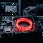
As artificial intelligence workloads scale and data transfer rates reach 800G, 1.6T, and beyond, traditional copper interconnects hit severe physical and thermal boundaries. Optical interconnects built on Silicon Photonics (SiPh) offer high bandwidth density, low latency, and superior power efficiency. However, integrating optics into compact transceivers and Co-Packaged Optics (CPO) architectures introduces a critical challenge: cumulative optical path loss.
To prevent link budget failure without resorting to energy-hungry electrical regeneration, data center architects rely on Indium Phosphide (InP) Semiconductor Optical Amplifiers (SOAs) for direct, low-latency signal amplification.
Understanding Coupling Loss in Semiconductor Optical Amplifiers SOAs
In optical packaging and photonic integrated circuits (PICs), coupling loss defines the proportion of optical power lost when transferring light into or out of a Semiconductor Optical Amplifier (SOA). Because an InP SOA operates by amplifying light via stimulated emission in a tight waveguide channel, any mismatch at the semiconductor interfaces directly degrades the net operational gain and system efficiency.
Identify the Main Sources of Loss
Achieving optimal optical throughput requires systematically isolating where signal attenuation occurs across the package interface:
- Mode Field Diameter (MFD) Mismatch: The optical mode size inside an InP SOA active waveguide is extremely small (~1 µm to 2 µm), whereas standard single-mode optical fiber (SMF-28) has an MFD of approximately 9 µm to 10 µm. Joining these two mismatched mode sizes without beam-shaping optics leads to severe coupling loss (>10 dB).
- Fresnel Reflections & Interface Reflection: Discontinuities in the refractive index between air ($n \approx 1.0$), glass/silica ($n \approx 1.45$), and InP semiconductor material ($n \approx 3.2–3.5$) cause backward reflections. These reflections not only reduce forward transmission power but can also induce unwanted laser instability and cavity resonance.
- Angular and Spatial Misalignment: Sub-micron axial ($X, Y, Z$) offsets or angular tilt between the fiber tip, coupling optics, and the InP chip facet rapidly decay the coupling efficiency.
- Polishing & Facet Degradation: Imperfections, micro-scratches, or tilt angle errors on the SOA chip facet scatter light and disrupt optimal spatial mode overlaps.
Improve Fiber-to-Chip Alignment
To bridge the mode-size gap and maximize coupling efficiency into InP SOAs, advanced packaging techniques and precision alignment methodologies are deployed:
- Lensed Fibers & Tapered Spot-Size Converters (SSCs):
- Lensed/Tapered Fibers: Lensed fiber tips focus incoming light to a sub-micron spot matching the SOA’s waveguide dimensions, reducing insertion loss down to < 2 dB per facet.
- Integrated Spot-Size Converters (SSCs): Monolithically integrated passive waveguide tapers on the InP chip expand the optical mode field prior to light exiting the chip, allowing better match with standard flat or angled physical contact (APC) fibers.
- Angled Facet & Anti-Reflection (AR) Coatings:
- Applying ultra-low reflectivity AR coatings ($R < 0.01\%$) to the InP chip facets minimizes Fresnel reflections.
- Tilting the SOA waveguide relative to the chip facet (typically angled by 7° to 10°) ensures residual reflected light escapes the waveguide mode, eliminating back-reflection interference.
- Active Sub-Micron Automated Alignment:
- During packaging assembly, automated piezo-driven alignment stages actively monitor optical output power while positioning fibers relative to the SOA chip. Machine-vision-guided robotic positioners achieve sub-micron alignment accuracy ($\pm 0.1 \ \mu\text{m}$) before laser welding or UV-cured epoxy bonding fixes the components in place.
Measure and Reduce Insertion Loss
Accurate optical loss characterization ensures that the SOA’s active optical gain exceeds total package insertion loss, yielding net optical gain for the system.
┌─────────────────────────────────────────┐
│ InP SOA Package Interface │
│ │
Input Power ──► │ [Facet Loss In] ──► [Active Gain] ──► [Facet Loss Out] │ ──► Amplified Output
(P_in) │ (~2 dB) (+20 dB) (~2 dB) │ (P_out)
└─────────────────────────────────────────┘
- Measuring Net Gain vs. Internal Single-Pass Gain:
- Internal Gain: The raw optical amplification provided by the pumped InP active region.
- Net Gain: The real-world gain measured outside the fiber pigtails or package terminals.
- Characterization Protocols:
- Continuous Wave (CW) Power Testing: High-precision optical power meters (OPMs) compare launch power ($P_{\text{in}}$) directly against amplified output power ($P_{\text{out}}$) across a swept wavelength spectrum.
- Noise Figure (NF) & ASE Measurement: Using an Optical Spectrum Analyzer (OSA) to measure Amplified Spontaneous Emission (ASE) noise spectral density, verifying that low-loss coupling keeps the noise figure near the theoretical lower limit (~5 dB to 7 dB).
- Target Optimization Goals: By combining angle-cleaved lensed fibers, optimized AR coatings, and thermal-expansion-matched sub-mounts (e.g., Copper-Tungsten or Aluminum Nitride), package insertion losses can be routinely reduced below 1.5 dB–2.0 dB per interface, unlocking maximum usable net gain for high-density 800G+ optical networks.
The Optical Loss Challenge in Silicon Photonic Integrated Circuits
Silicon photonic integrated circuits (PICs) excel at routing and modulating light, but silicon’s indirect bandgap prevents it from efficiently emitting light. Routing external laser signals into SiPh chips introduces significant insertion and propagation losses:
- Mode-Mismatch & Coupling Loss: Interfacing standard single-mode fiber (SMF) or external laser diodes with sub-micron silicon waveguides creates a spatial mode mismatch. Edge couplers and vertical grating couplers routinely introduce insertion losses ranging from 1.5 dB to over 4 dB per interface.
- Passive Component Attenuation: On-chip optical components—including ring modulators, Mach-Zehnder Interferometers (MZIs), arrayed waveguide gratings (AWGs), and power splitters—accumulate transmission losses across the circuit.
- Connectors and Multiplexing: Multi-channel WDM (Wavelength Division Multiplexing) links incur loss at every multiplexing and fiber-to-chip connection step, reducing the total Optical Modulation Amplitude (OMA) at the receiver end.
When cumulative loss exceeds the launch power budget, signal-to-noise ratios degrade, bit error rates (BER) rise, and transceivers fail to hit reach requirements.

How InP SOAs Compensate for Loss in the Optical Domain
A Semiconductor Optical Amplifier (SOA) is an optoelectronic device, also known as one of the SOAs used in photonic systems, that amplifies an incoming optical signal directly through stimulated emission within an InP gain medium—eliminating the need for Optical-Electrical-Optical (O-E-O) conversion.
Optical Input (P_in) ──► [ Antireflection Coating ] ──► [ InP Active Gain Region ] ──► [ Amplified Output (P_out) ]
▲
│
Pumping Current
Key Technical Advantages of SOAs in Transceiver Architectures
- Direct All-Optical Amplification: SOAs amplify optical signals across the O-band (1310 nm) and C-band (1550 nm), providing broad gain bandwidth while preserving signal modulation formats without introducing conversion latency.
- Compact Footprint: Unlike bulky fiber-based amplifiers, InP SOAs feature tiny chip-scale footprints that allow for direct integration into 14-pin butterfly packages, TO-cans, or hybrid chip-on-carrier (CoC) assemblies.
- Wide Optical Bandwidth & High Gain: Provides optical gain across wide spectral windows, boosting multiple multiplexed channels simultaneously.
- Low Polarization Dependency: Features low Polarization Dependent Gain (PDG), ensuring consistent signal amplification regardless of incoming light polarization state.
SOA vs. EDFA: Selecting the Right Amplifier for Compact Form Factors
| Feature / Metric | Semiconductor Optical Amplifier (SOA) | Erbium-Doped Fiber Amplifier (EDFA) |
| Physical Size | Microscopic chip / compact package | Spooled fiber reel + pump laser (Large) |
| Integration | On-chip, co-packaged, or transceiver module | Standalone rack / benchtop equipment |
| Wavelength Coverage | Flexible InP bandgap design (1310nm O-band & 1550nm C-band) | Primarily C-band (1530–1565nm) and L-band |
| Power Consumption | Low bias current (compact electrical envelope) | High pump laser power required |
| Primary Use Case | Transceivers, CPO, PIC loss compensation, optical switching | Long-haul telecommunications & fiber backbones |
Application Architectures: Where to Place SOAs in High-Speed Links
SOAs fulfill distinct roles depending on where they are deployed along the optical transmission path:
[ External Light Source ] ──► [ Silicon Photonic Chip ] ──► [ SOA (Booster) ] ──► Fiber Link │
▼
Receiver ◄── [ SOA (Preamplifier) ] ◄── Fiber Link ◄──────────────┘
- Booster Amplifier (Post-Amplification): Positioned immediately after the silicon photonic modulator or chip interface to boost the launch power before light enters the transmission fiber, overcoming initial coupling and modulation losses.
- In-Line Amplifier: Placed at mid-span optical nodes to restore attenuated signals in campus-level data center interconnects without O-E-O conversion.
- Preamplifier (Pre-Receiver Amplification): Placed directly before photodetectors at the receiver end to boost weak signals above the thermal noise floor of transimpedance amplifiers (TIAs), significantly improving receiver sensitivity.
Inphenix InP SOA Solutions for Next-Generation Datacom
Inphenix manufactures high-performance InP Semiconductor Optical Amplifiers designed to meet the rigorous demands of high-density datacom, optical sensing, and test-and-measurement environments:
- Custom Wavelength Coverage: Available across critical datacom spectrums including 1310 nm (O-band) and 1550 nm (C-band).
- Low Noise Figure & Low Reflection: High optical gain with low noise figure (NF) and minimal facet reflectivity for stable operation in sensitive optical networks.
- Flexible Packaging & OEM Customization: Offered in industry-standard 14-pin butterfly packages with integrated TEC/thermistor control, or customized chip-on-carrier form factors for direct hybrid PIC integration.